Sequential Logic:
Before we covered how to create complicated combinational logic that eventually lead to the creation of an ALU (Arithmetic Logic Unit), the most central part of a processor. These were however all operations that occur (nearly) instantly after the right input combinations were given. In computing we need to be able to store variables to make the right computations to them, and we also need to be able to store the program that the processor will use to execute the right instructions. In order to do this we need sequential logic, or logic that not only depends on the current input, but the previous output or state of the device.
The Digital Latch:
The most simple devices in digital electronics that store information from a previous state, are latches, and the easiest one to implement using gate or transistor level design is the SR-Latch, or Set/Reset Latch, as shown below.
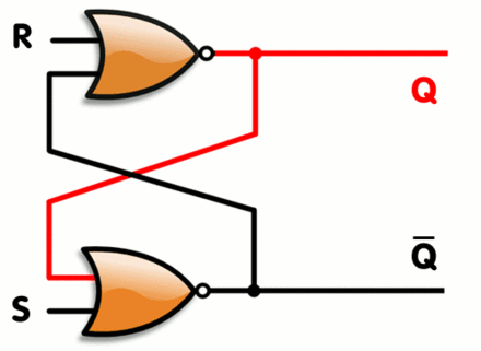
The common design element that allows the previous output of the device to dictate the current one is feedback. Below is a truth table that shows how each input and the previous state affects the outcome. Note how because the output of the SR latch is connected back into the input, the output of the latch now can stay in the same state when both inputs are low. Whenever the input is high on the set pin, the output becomes low, and the opposite is true of the reset pin. When both inputs are high however, something called a race condition occurs. This is a very important concern in digital electonics where the output of the device becomes unpredictable due to competing output assertions. The reason it is called a race condition is because both inputs are in a race to make their output assertion first. There are various ways to add complexity to the design to overcome this problem that are beyond the scope of these posts, remember I’m mostly interested in programmers becoming more aware of how their computers and their software work behind the scenes.
| SR latch operation[13] | ||||||||
|---|---|---|---|---|---|---|---|---|
| Characteristic table | Excitation table | |||||||
| S | R | Qnext | Action | Q | Qnext | S | R | |
| 0 | 0 | Q | hold state | 0 | 0 | 0 | X | |
| 0 | 1 | 0 | reset | 0 | 1 | 1 | 0 | |
| 1 | 0 | 1 | set | 1 | 0 | 0 | 1 | |
| 1 | 1 | X | not allowed | 1 | 1 | X | 0 | |
The Digital Flip-Flop
Yes, this device has a somewhat silly name, (engineers are very silly people deep down inside in the best way possible), but it is arguably one of the most important digital devices there are. What seperates a flip flop device from a latch, is that inputs and states are asserted synchronously at the edge of a clock signal. Without getting into too much detail, this allows digital systems to be easilier be synchronized to a shared system clock. In computers this is extremely important since so many different components have to work together so quickly. This becomes more clear when examining this signal pattern below for one of the most used sequential devices in digital electronics, the D-Flip-Flop.
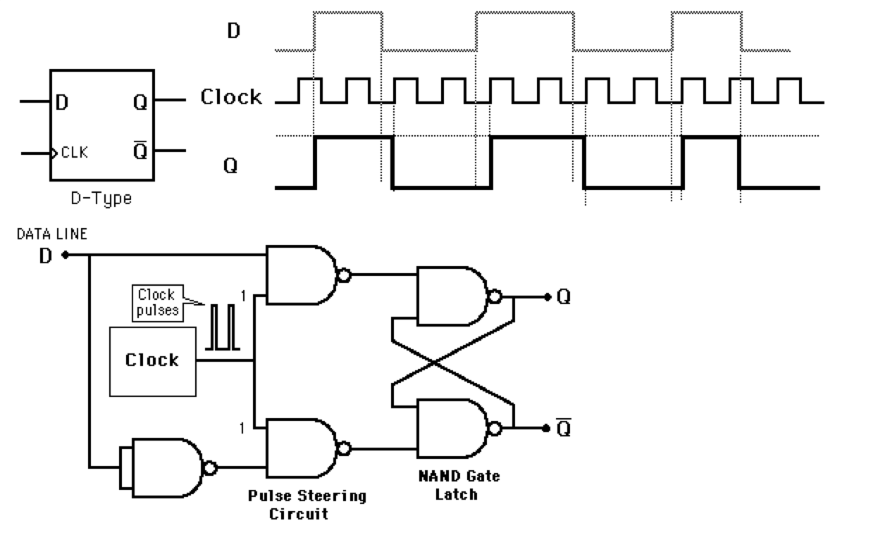 From hyperphysics,
The D flip-flop tries to follow the input D but cannot make the required transitions unless it is enabled by the clock. Note that if the clock is low when a transition in D occurs, the tracking transiton in Q occurs at the next upward transition of the clock.”
So essentially, the device holds onto whatever the digital signal the input pin “D” has when the clock edge is reached. This design can be altered with some slight reconfigurations so that the output is only altered when both the clock and and a write-enable input is given. This creates what is one of the most important devices in computer architecture, the Register
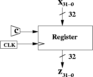
Registers
From wikiBooks on Digital Circuits
Registers are groups of flip-flops, where each flip-flop is capable of storing one bit of information. An n-bit register is a group of n flip-flops. The basic function of a register is to hold information in a digital system and make it available to the logic elements for the computing process.
There generally two kinds of registers, serial registers and parallel registers. Serial Registers as the name suggests either take in data in one serial line, or send it back out in a serial line, or both. Parallel registers do the same with parallel lines equaling the number of bits they store. Typically in processor design they are parallel registers on both the input and out.
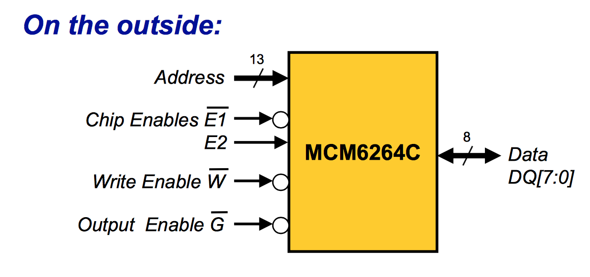
RAM
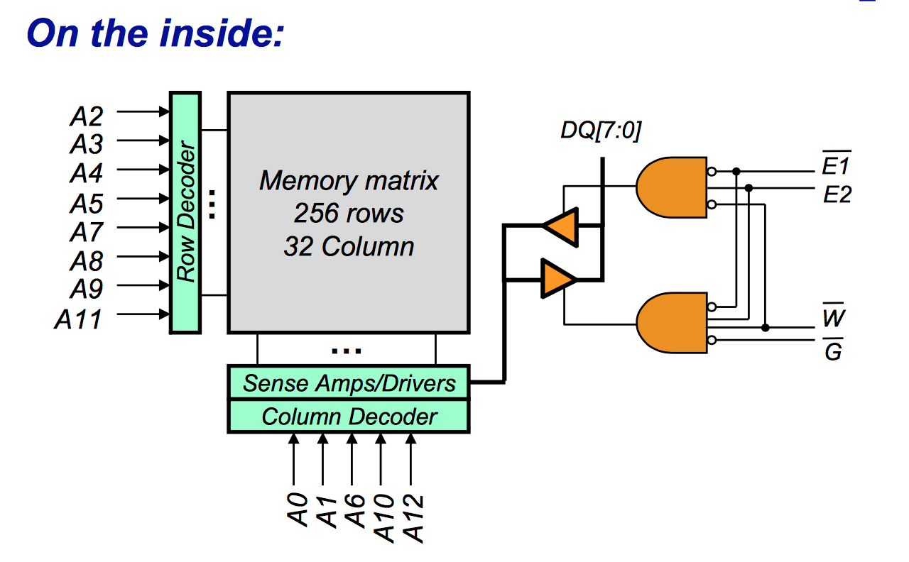
A RAM cell is not very different from a register in that it uses feedback elements to hold an output state and to write to it when desired. The only difference is that you need to be able to stack them in rows and resolve how to read and write to the corret element when desired. Note that the cell design below is just for one bit of storage, for modern processors the bus is 64-bits wide which means each RAM element would have 64 of these cells arranged in each row so that you whenever you read or write to RAM it is in 64-bit or 4-Byte words.
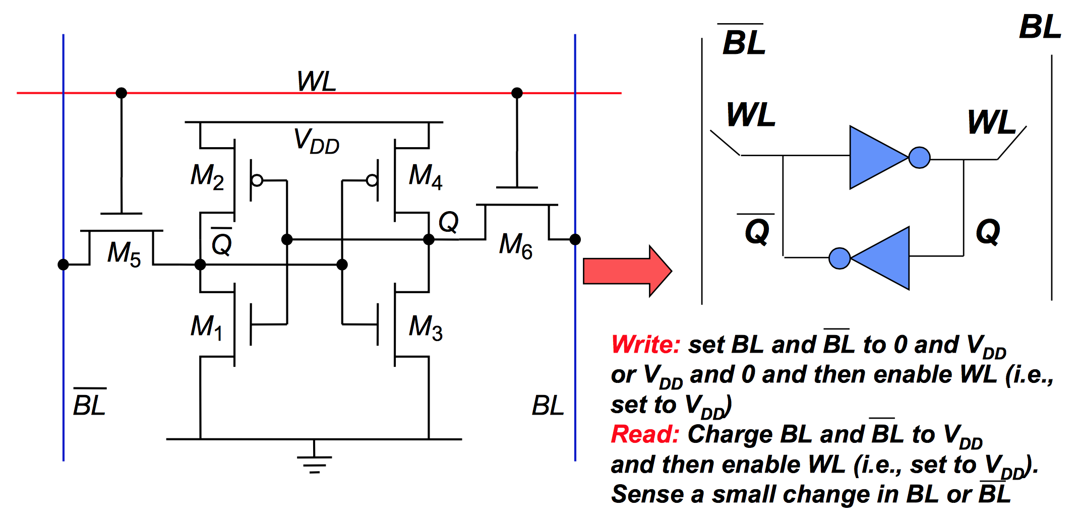
In most cases each word will also be arranged in columns to reduce the number of address selection lines needed to choose which RAM cells are written to and read from. Remember decoders? If we have an 8-bit system bus that directs an 8 bit decoder, that decoder can now select 256 rows of cells to read from, and if we combine that with a column decoder of 8 bits in width means that we get 256 columns of cells to chose from. Together that means 65,536 Bytes of RAM, such storage, wow. The only control inputs left in order to have full control over a RAM cell, are a clock pin to keep things synchronized, a chip enable (E) in the likely case we are using more than one RAM module and we need to choose which one is being used, a Write Enable ![]() to indicate we want to write to the cell at the given address, and an Output Enable (O,or G) which is there so that we are only outputing one module to the bus at the same time.
to indicate we want to write to the cell at the given address, and an Output Enable (O,or G) which is there so that we are only outputing one module to the bus at the same time.
And That’s it really for storage elements. Now that we know how to make complex combinational circuits and complex sequential circuits we can design a large portion of the devices necessary in processors. Tune in next time where we’ll go over the basics of how to coordinate all the data buses in a processor that routes data from various storage elements, to/from arithmetic and data modulation elemetns to/from the peripheral bus.
Refrences
- My own professional and academic experience as an Electrical Engineer
- Hyperphysics:
- MIT OCW: Introduction to Digital Systems
