Introduction
Switching my primary career focus from Electrical Engineering to Software Development I’m told I have a pretty unique perspective on working with computing systems. I tend to agree, although I wish I had come to realize that I would be more fulfilled writing software than working with computer hardware, I do have an appreciation for the knowledge of how these lines of code become binary sequences that tell a computer how to perform the desired actions that a program will give it.
Abstraction
The reason that many software developers don’t know these details is mostly due to abstraction. One reason we abstract things is so that we can focus on the correct scope of actions so that we get the desired work done with minimal effort. If we didn’t, we’d probably still be loading decks of punchcards into our computers to tell them what it is we want them to do; not ideal. Fortunately as our computers’ capabilities evolved, how we interact with them has evolved with them, and this is largely due to continuing abstraction. In this series of blog posts I hope to bridge the gap of knowledge between the software developer writing code for his computers and how that code eventually becomes the correct sequence of binary signals stored as programs, and how computers convert that program into the desired outputs they were programmed for. I will start by showing how transistors work, and how they are used to design basic digital circuits, then I will show how these basic digital circuits form the basic components of a computer such as memory, computational units and data path, and then finally I will show how programs are turned into binary instructions for these computers to work with.
The Transistor
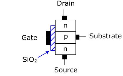
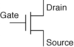
We’ll begin this exploration for how computers turn code into the desired output, through a bottom up approach, by starting with the Transistor. Just how the building blocks of matter are the atoms they are composed of, the building blocks of digital systems are the transistor. Transistors are formed out of semiconductors, usually differently concentrated silicon. Due to silicon’s atomic nature it can be induced to have slight electrical biases, that is to prefer positive or negative charges at extremely minute levels. N-type silicon is silicon that has slightly more electrons within the substrate than a neutral charge, and vice versa for p-type, with what we call holes. When these types of silicon are combined in the way shown in the diagram below we get what’s called a MOSFET – Metal Oxide Substrate Field Effect Transistor, the type of transistors most commonly found within CPU’s.
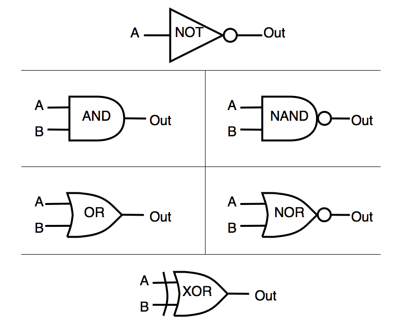
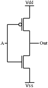
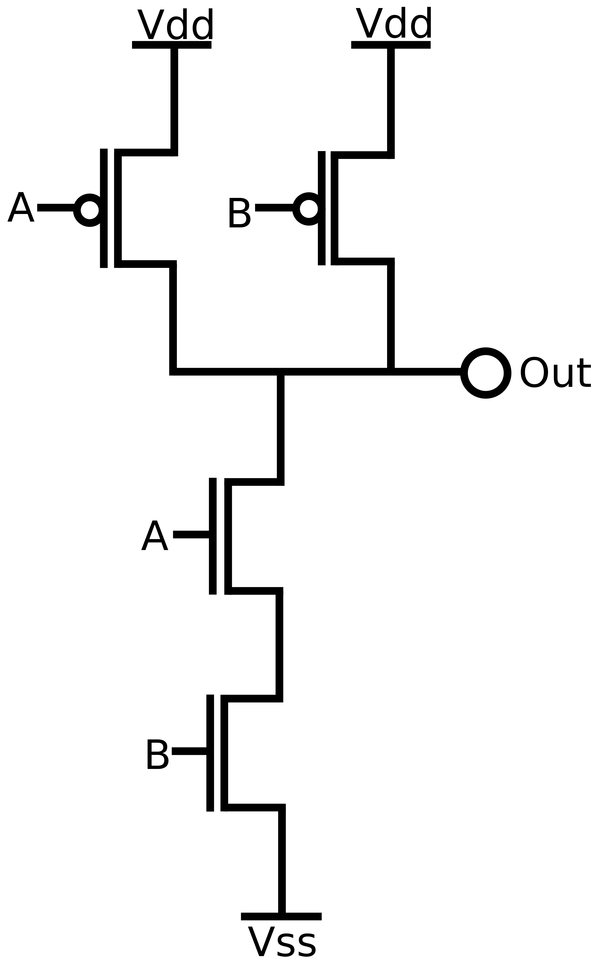
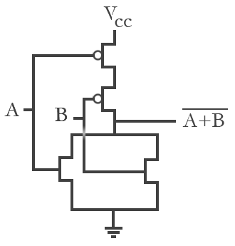
These gates can all be made by using transistors in certain design patters that can be repeated for each and every logic gate required. They are shown below for the AND, OR, NOT gates.
Designing Digital Circuits
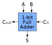
The way we design digital logic circuits is by analyzing truth tables. When we design logical circuits we know the end result of the logic circuit that we want, and we know the input to that circuit that should give us that result. We organize this information with truth tables, like the one below, to help us visualize the combinational logic for the circuit. To show how computation can be performed with logic circuits we’ll go through the design for a single bit adder. Below there’s the block diagram showing the inputs and outputs for a full adder. You need the two bits to be added ‘A’ & ‘B’, a Carry-in ‘Cin’ (more on this later), a Sum output ‘S’, and Carry-out (Cout). You may be confused by the carry input and outputs, but bare with me. The carry out is there to represent how we have to carry a number between digits while adding. Just like in the decimal number system we have to carry a ‘1’ over to the next digit if the sum exceeds ‘9’ on that digit, binary is just the same. The only difference is that in a binary number system we carry the ‘1’ if the sum goes beyond just ‘1’. The carry in bit is just the input that accepts the carry out from the previous digit so that it gets accounted for in the sum.
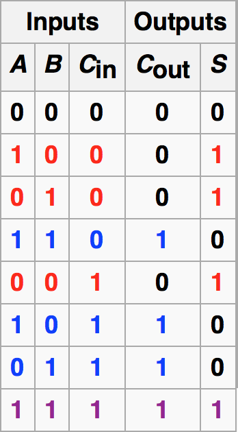
Now that we have the desired truth table its time to deconstruct the logic we need to make this function work as intended. We usually do this by examining which outputs have a ‘1’ and noting what combination of inputs give us this output. The combination of inputs that give a ‘true’ output for the sum bit are colored red, while the carry out bit is colored blue, and the one combination that makes both true is purple. If we represent AND’ed inputs as a products symbolically, OR’ed inputs as a sum, and NOT’ed inputs as a bar over the input letter, we get this equation for the Sum bit and the Carry bit. The circle with the cross is the XOR function and we arrive at its use by noting which bits are different at the inputs, and they are preferable to AND or OR gates because they usually require fewer transistors.
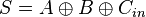

This equation now can tell us what the logic circuit will look like. If we examine each function in order we see that for the sum, A XOR B XOR Cin = Sum. For Cout we see that A XOR B, then AND’ed with Cin, then OR’ed with A AND B.


Excellent post, very informative, and I found it to be very clear. That said, I imagine some readers could benefit from an expansion of your paragraph on transistors, perhaps an explanation of the schematics you put up. ‘E.g., semi-conductors have properties that are affected by electric current — so if you can send a current to divert electrical flow from a second circuit, then you have effectively input ~5mV, and output ~1mV — which exactly models a NOT gate.’ Again, really like the post!
LikeLike